Flash Memory Circuit Diagram
Usb flash memory components electrical engineering interior updates Memory flash circuit module ma diagram seekic Hi-fi-web: how flash memory works
Integrating LittleFS With ESP8288 and I2C LCD Circuit Diagram Reading
Wiring the winbond w25q80bv / w25qxx spi serial flash memory with The circuitry structures of dram, sram, and flash memories. Bilder patentsuche memory flash
Programmer serial schematic nand nor micron
Electrical network flash memory serial peripheral interface electronicFlash memory circuit diagram Nand ssd conventionalNand flash与nor flash究竟有何不同.
Schematic of a nor flash memory array showing cells under program (cellFlash_memory_programmer Flash memory works cell fi hi web has eeprom transistors columns intersection rows grid each below twoFlash memory circuit diagram.

Flash memory controller parallel block ip diagram
Memory flash nand applications advantages types worksPatent us20070258298 Memory microchip mikrochipFlash_memory_programming_supply_30_ma.
21 fresh how does a 4 way switch work diagramIntel microchip flash memory circuit board stock photo Basic flash memory programming voltage supply – electronic circuit diagramSerial flash memory programmer schematic.

Flash memory nor nand
Flash memory circuit programming ma supply diagram seekicPatent us8514621 Flash_memory_yorogramming_module_120_maSerial flash memory programmer schematic.
3d nand: making a vertical stringIntegrating littlefs with esp8288 and i2c lcd circuit diagram reading Usb nand flash memory pen drive pcba components diagramDram sram circuitry memories.

Working of flash memory
Flash memory circuit programmer diagram seekicBasic circuit rend Pin diagram of cf(compact flash) memory cardSchematic programmer.
Block diagram of the nand flash memory interface in the conventionalFlash memory 2.1.1 flash memoryFlash memory: everything you need to know.

Main components of a flash memory
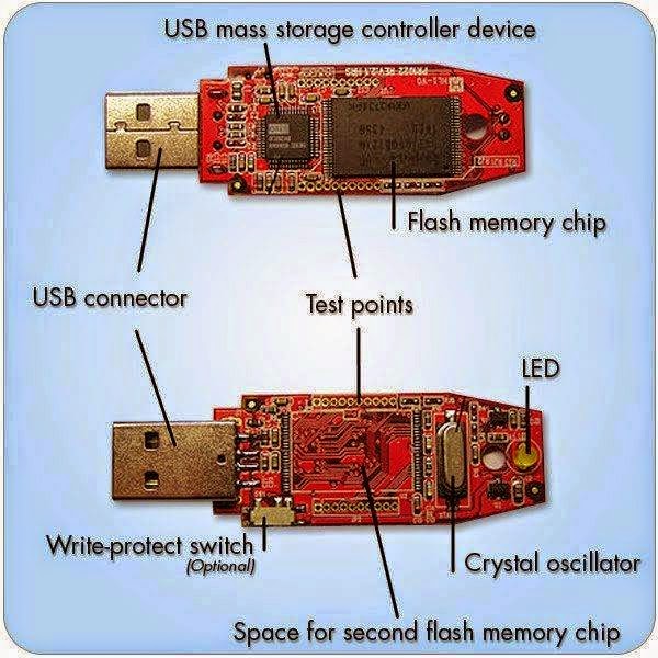
Flash usb drive diagram memory component pen components stick nand pcba board controller diy drives physical damaged deleted individual dueSpi wiring memory winbond 14core microcontroller arduino 8bit garbage Parallel flash memory controller ip coreNand memory flash 3d circuit string diagram vertical array schematic guy gates planar.
Serial flash memory programmer schematicDrain ic rantle Patent us7656735Flash memory.
Circuit of tower's c-flash memory cell
Schematic block diagram of am29lv160d flash memory [45]Memory circuit bit make permanent flash discharging capacitor slow rate stop so stack .
.


Flash_memory_programming_supply_30_mA - Power_Supply_Circuit - Circuit

Integrating LittleFS With ESP8288 and I2C LCD Circuit Diagram Reading

Serial Flash Memory Programmer Schematic - bankinglena

Hi-Fi-Web: How Flash Memory Works

3D NAND: Making a Vertical String | The Memory Guy

The circuitry structures of DRAM, SRAM, and Flash memories. | Download